- 您现在的位置:买卖IC网 > Sheet目录3871 > PIC18F4682T-I/ML (Microchip Technology)IC PIC MCU FLASH 40KX16 44QFN
PIC18F46J50 FAMILY
DS39931D-page 138
2011 Microchip Technology Inc.
TABLE 10-4:
SUMMARY OF REGISTERS ASSOCIATED WITH PORTA
RA5/AN4/SS1/
HLVDIN/RCV/
RP2
RA5
0
O
DIG
LATA<5> data output; not affected by analog input.
1
I
TTL
PORTA<5> data input; disabled when analog input is
enabled.
AN4
1
I
ANA A/D Input Channel 4. Default configuration on POR.
SS1
1
I
TTL
Slave select input for MSSP1.
HLVDIN
1
I
ANA High/Low-Voltage Detect external trip point reference input.
RCV
1
I
TTL
External USB transceiver RCV input.
RP2
1
I
ST
Remappable Peripheral Pin 2 input.
0
O
DIG
Remappable Peripheral Pin 2 output.
OSC2/CLKO/
RA6
OSC2
x
O
ANA Main oscillator feedback output connection (HS mode).
CLKO
x
O
DIG
System cycle clock output (FOSC/4) in RC and EC Oscillator
modes.
RA6
1
I
TTL
PORTA<6> data input.
0
O
DIG
LATA<6> data output.
OSC1/CLKI/RA7
OSC1
1
I
ANA Main oscillator input connection.
CLKI
1
I
ANA Main clock input connection.
RA7
1
I
TTL
PORTA<6> data input.
0
O
DIG
LATA<6> data output.
Name
Bit 7
Bit 6
Bit 5
Bit 4
Bit 3
Bit 2
Bit 1
Bit 0
Reset
Values
on Page
PORTA
RA7
RA6
RA5
—
RA3
RA2
RA1
RA0
LATA
LAT7
LAT6
LAT5
—
LAT3LAT2LAT1LAT0
TRISA
TRIS7
TRIS6
TRISA5
—
TRISA3
TRISA2
TRISA1
TRISA0
ANCON0
PCFG7(1) PCFG6(1) PCFG5(1)
PCFG4
PCFG3
PCFG2
PCFG1
PCFG0
CMxCON
CON
COE
CPOL
EVPOL1
EVPOL0
CREF
CCH1
CCH0
CVRCON
CVREN
CVROE
CVRR
r
CVR3
CVR2
CVR1
CVR0
Legend:
— = unimplemented, read as ‘0’, r = reserved. Shaded cells are not used by PORTA.
Note 1:
These bits are only available on 44-pin devices.
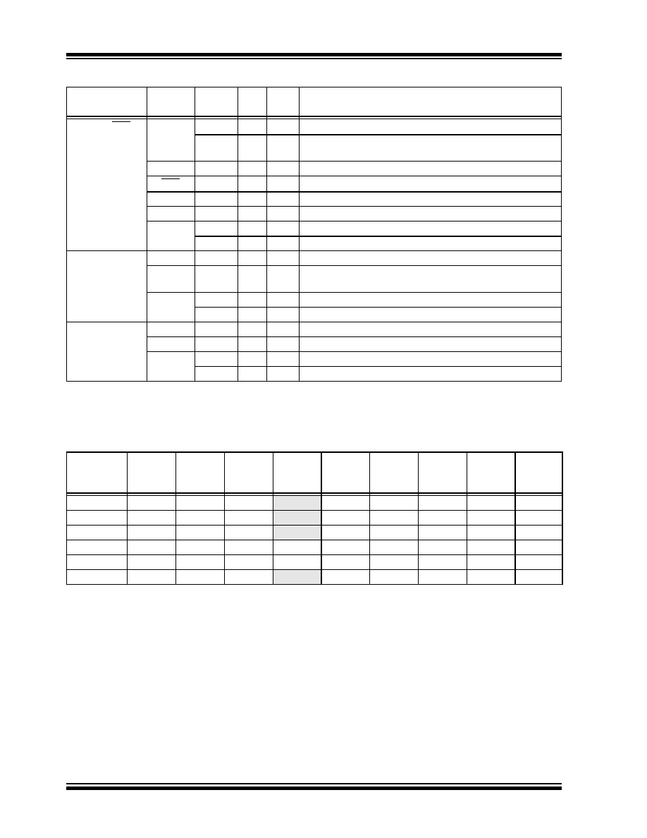
TABLE 10-3:
PORTA I/O SUMMARY (CONTINUED)
Pin
Function
TRIS
Setting
I/O
Type
Description
Legend:
DIG = Digital level output; TTL = TTL input buffer; ST = Schmitt Trigger input buffer; ANA = Analog level
input/output; x = Don’t care (TRIS bit does not affect port direction or is overridden for this option)
Note 1:
This bit is only available on 44-pin devices.
发布紧急采购,3分钟左右您将得到回复。
相关PDF资料
PIC24HJ128GP306T-I/PT
IC PIC MCU FLASH 128KB 64TQFP
PIC24FJ96GA008T-I/PT
IC PIC MCU FLASH 96KB 80TQFP
PIC24FJ64GA010T-I/PT
IC PIC MCU FLASH 64KB 100TQFP
PIC24FJ64GA008T-I/PT
IC PIC MCU FLASH 64KB 80TQFP
PIC18LF4450T-I/PT
IC PIC MCU FLASH 8KX16 44TQFP
PIC18LF2450T-I/ML
IC PIC MCU FLASH 8KX16 28QFN
PIC16F1937-I/ML
IC PIC MCU FLASH 512KX14 44-QFN
PIC18F25K20-E/ML
IC PIC MCU FLASH 16KX16 28-QFN
相关代理商/技术参数
PIC18F4682T-I/PT
功能描述:8位微控制器 -MCU 80KB FL 3328bytes RAM 36I/O RoHS:否 制造商:Silicon Labs 核心:8051 处理器系列:C8051F39x 数据总线宽度:8 bit 最大时钟频率:50 MHz 程序存储器大小:16 KB 数据 RAM 大小:1 KB 片上 ADC:Yes 工作电源电压:1.8 V to 3.6 V 工作温度范围:- 40 C to + 105 C 封装 / 箱体:QFN-20 安装风格:SMD/SMT
PIC18F4685-E/ML
功能描述:8位微控制器 -MCU 96KB 3328 RAM w/ECAN RoHS:否 制造商:Silicon Labs 核心:8051 处理器系列:C8051F39x 数据总线宽度:8 bit 最大时钟频率:50 MHz 程序存储器大小:16 KB 数据 RAM 大小:1 KB 片上 ADC:Yes 工作电源电压:1.8 V to 3.6 V 工作温度范围:- 40 C to + 105 C 封装 / 箱体:QFN-20 安装风格:SMD/SMT
PIC18F4685-E/P
功能描述:8位微控制器 -MCU 96KB 3328 RAM w/ECAN RoHS:否 制造商:Silicon Labs 核心:8051 处理器系列:C8051F39x 数据总线宽度:8 bit 最大时钟频率:50 MHz 程序存储器大小:16 KB 数据 RAM 大小:1 KB 片上 ADC:Yes 工作电源电压:1.8 V to 3.6 V 工作温度范围:- 40 C to + 105 C 封装 / 箱体:QFN-20 安装风格:SMD/SMT
PIC18F4685-E/PT
功能描述:8位微控制器 -MCU 96KB FL 3328bytes RAM 36I/O RoHS:否 制造商:Silicon Labs 核心:8051 处理器系列:C8051F39x 数据总线宽度:8 bit 最大时钟频率:50 MHz 程序存储器大小:16 KB 数据 RAM 大小:1 KB 片上 ADC:Yes 工作电源电压:1.8 V to 3.6 V 工作温度范围:- 40 C to + 105 C 封装 / 箱体:QFN-20 安装风格:SMD/SMT
PIC18F4685-I/ML
功能描述:8位微控制器 -MCU 96KB 3328 RAM w/ECAN RoHS:否 制造商:Silicon Labs 核心:8051 处理器系列:C8051F39x 数据总线宽度:8 bit 最大时钟频率:50 MHz 程序存储器大小:16 KB 数据 RAM 大小:1 KB 片上 ADC:Yes 工作电源电压:1.8 V to 3.6 V 工作温度范围:- 40 C to + 105 C 封装 / 箱体:QFN-20 安装风格:SMD/SMT
PIC18F4685-I/ML
制造商:Microchip Technology Inc 功能描述:IC 8BIT MCU PIC18F 40MHZ QFN-44 制造商:Microchip Technology Inc 功能描述:IC, 8BIT MCU, PIC18F, 40MHZ, QFN-44
PIC18F4685-I/P
功能描述:8位微控制器 -MCU 96KB 3328 RAM w/ECAN RoHS:否 制造商:Silicon Labs 核心:8051 处理器系列:C8051F39x 数据总线宽度:8 bit 最大时钟频率:50 MHz 程序存储器大小:16 KB 数据 RAM 大小:1 KB 片上 ADC:Yes 工作电源电压:1.8 V to 3.6 V 工作温度范围:- 40 C to + 105 C 封装 / 箱体:QFN-20 安装风格:SMD/SMT
PIC18F4685-I/P
制造商:Microchip Technology Inc 功能描述:8-Bit Microcontroller IC